FPGA vs ASIC: The Difference Between LEGO and a Model Kit
Why did Bitcoin miners switch from GPUs to ASICs? The battle between flexibility (FPGA) and extreme efficiency (ASIC).

Why did Bitcoin miners switch from GPUs to ASICs? The battle between flexibility (FPGA) and extreme efficiency (ASIC).
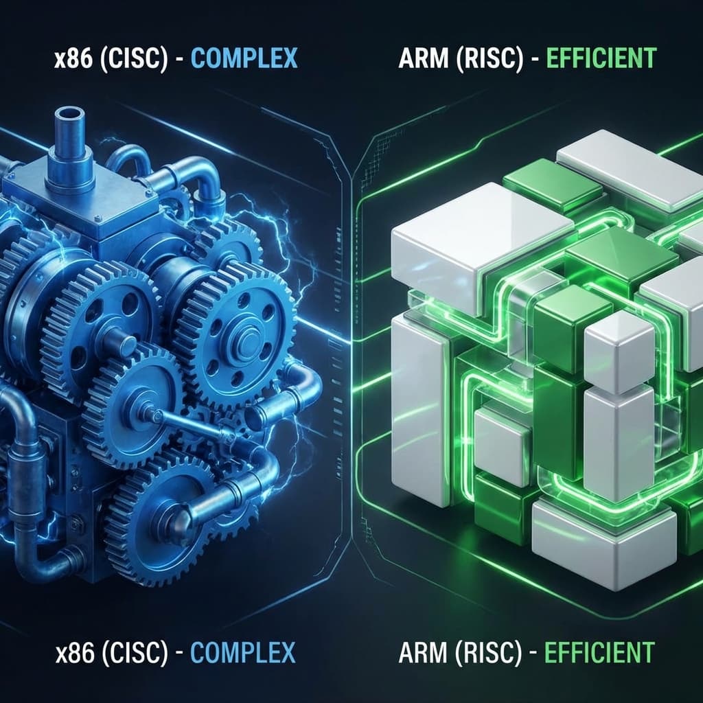
Why does MacBook battery last long? Should I use AWS Graviton? A deep dive into the philosophy of CISC (Complex) vs RISC (Simple) architectures.

The gold mine of AI era, NVIDIA GPUs. Why do we run AI on gaming graphics cards? Learn the difference between workers (CUDA) and matrix geniuses (Tensor Cores).

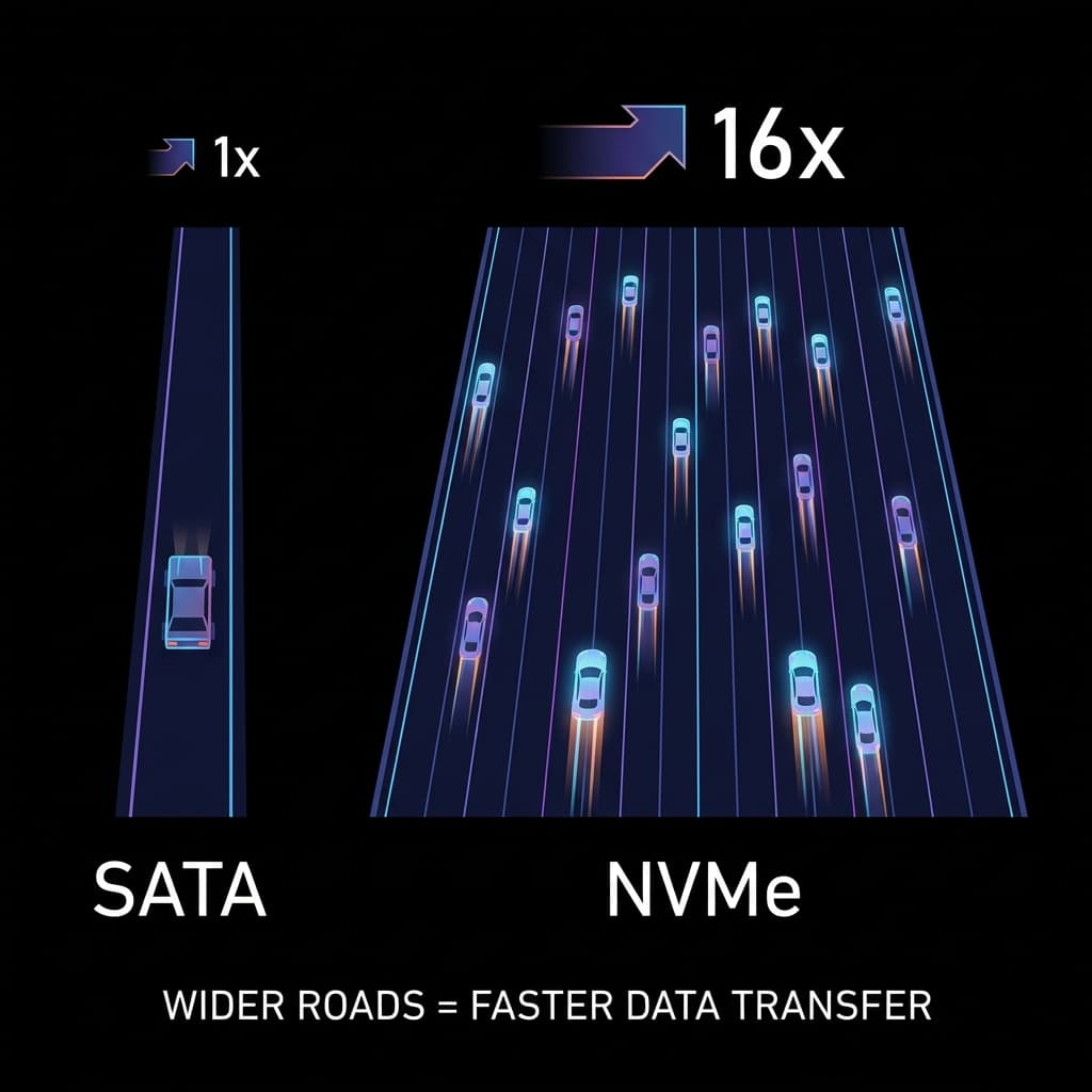
Bought a fast SSD but it's still slow? One-lane country road (SATA) vs 16-lane highway (NVMe).

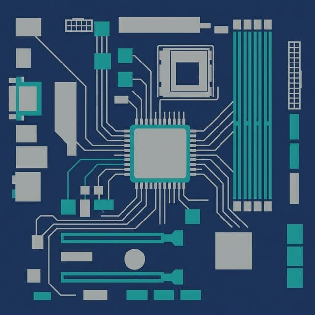
I thought the motherboard was just a board to plug things into. Then I learned what a chipset does.

Early Bitcoin was mined with CPUs. Then GPUs took over. Then suddenly, weird machines called 'Miners (ASICs)' appeared everywhere.
Why not just use regular computers? Why build dedicated machines?
To answer this, I dove into the two titans of semiconductor design: FPGA and ASIC. At first, I thought "they're both chips, what's the difference?" But I quickly learned they're as different as LEGO blocks and injection-molded plastic toys.
Understanding this difference unlocked why Tesla builds their own FSD chips, why Google developed TPUs, and why Bitcoin mining companies go bankrupt when algorithms change.
When I first encountered FPGA and ASIC, I honestly couldn't tell them apart. They're both "semiconductor chips" that "perform calculations," so what's the big deal?
But as I dug deeper, I realized the way they're made is fundamentally different.
FPGA lets you reprogram the internal circuits of an already-manufactured chip. The chip itself stays the same, but you can change how the logic gates (AND, OR, NOT, etc.) are connected using software.
ASIC, on the other hand, means you design circuits from scratch and bake them into silicon wafers. Once made, that's it. No modifications.
Once I understood this, the phrase "FPGA is general-purpose, ASIC is custom-made" clicked.
FPGA (Field-Programmable Gate Array) is exactly what the name suggests: a chip "Programmable in the Field" (meaning after manufacturing).
Inside an FPGA, you'll find LUTs (Look-Up Tables)—small chunks of memory that can store combinational logic functions. A typical FPGA has tens of thousands to millions of these LUTs.
For example, a 4-input LUT can store a truth table like this:
| A | B | C | D | Output |
|---|---|---|---|---|
| 0 | 0 | 0 | 0 | 0 |
| 0 | 0 | 0 | 1 | 1 |
| ... | ... | ... | ... | ... |
These LUTs are grouped into CLBs (Configurable Logic Blocks), which are interconnected by a "Routing Fabric"—a mesh of programmable wires.
So an FPGA is essentially "pre-made LEGO blocks (LUTs) and connectors (Routing) that you assemble to build your desired circuit."
FPGAs are programmed using HDL (Hardware Description Language)—typically Verilog or VHDL.
Here's a simple 2-input AND gate in Verilog:
module and_gate(
    input wire a,
    input wire b,
    output wire y
);
    assign y = a & b;
endmodule
When you load this code onto an FPGA, one of its LUTs becomes a circuit that "takes inputs a and b, and outputs their AND result."
"Writing code changes the chip's circuitry"—that blew my mind. As a software developer, I thought "code lives in memory," but with FPGAs, code becomes hardware circuits.
Think of an FPGA as a Swiss Army Knife:
Same with FPGAs:
So where are FPGAs actually used? From my research:
Bottom line: FPGAs thrive "where flexibility is critical."
ASIC (Application-Specific Integrated Circuit) is a chip "dedicated to one specific task."
Bitcoin miners (like Antminer) are classic ASICs. These chips do absolutely nothing except SHA-256 hashing. They can't run Windows or play Minesweeper.
But for that one task—SHA-256 computation—they're 100x faster than FPGAs and use 1/100th the power.
The ASIC creation process is completely different from software development. Here's what I learned:
This process takes at least 6 months to 2 years. And once you tape out, there's no going back.
If there's a bug in your design? You scrap all the chips and start over. That's why people say "one bad chip design can bankrupt a company."
ASIC design involves NRE (Non-Recurring Engineering) costs—one-time upfront expenses including:
The smaller the process node, the more expensive masks become:
So designing a 7nm ASIC requires $50M–$500M in NRE alone. Obviously, individuals and small companies can't afford this.
But if you stamp out 1 million chips, unit cost drops to $1–$10. That's the economics of ASICs.
Let me give another analogy for FPGA vs ASIC:
This reminds me of my own product development. I started with a "general framework (Django)" for quick MVP, then migrated to "optimized microservices (Go)" later. It's exactly the same FPGA → ASIC progression.
This was what got me interested in FPGA vs ASIC in the first place. Here's how Bitcoin mining evolved:
Watching this evolution taught me: "general → specialized" is the inevitable path of technology. Whether it's software, hardware, or business—everything follows the same trajectory.
Here's my decision framework:
Let's compare the same operation implemented in software vs FPGA.
def multiply_add(a, b, c):
    result = a * b + c
    return result

# Execution: CPU sequentially processes instructions
# 1. Calculate a * b
# 2. Add c to result
# 3. Return
module multiply_add(
    input wire [31:0] a,
    input wire [31:0] b,
    input wire [31:0] c,
    output wire [31:0] result
);
    wire [31:0] product;
    assign product = a * b;
    assign result = product + c;
endmodule

// This isn't "instructions"—it's a "circuit structure."
// a * b and + c are implemented as actual hardware,
// completing in 1–2 clock cycles.
See the difference? Software is "telling the CPU what to do," while FPGA is "the chip itself becomes the circuit that does the operation."
That's why FPGAs have extremely low latency. Input signals arrive, and results come out in just a few clock cycles. Software involves function calls, memory access, cache misses—hundreds of cycles.
Studying FPGA vs ASIC reinforced a key lesson: "Technology choices are ultimately about economics."
| Aspect | FPGA | ASIC |
|---|---|---|
| Analogy | LEGO Blocks (Rebuildable) | Injection Mold (Fixed) |
| Flexibility | High (Modify anytime) | None (Done is done) |
| Initial Cost | Low ($10K–$100K) | Very High ($5M–$500M) |
| Unit Price | Expensive ($100–$10K) | Cheap ($1–$10 at scale) |
| Power Efficiency | Medium | Best (10–100x better than FPGA) |
| Development Time | Short (weeks to months) | Long (6 months to 2 years) |
| Best For | Prototypes, low volume, algorithm changes | Mass production, performance/power critical, fixed algorithm |
To me as a developer, FPGAs feel like software ("just rewrite if it breaks"), while ASICs feel like hardware manufacturing ("one bug and the company goes under").
I now understand why Tesla builds their own FSD chips—Intel CPUs and NVIDIA GPUs (general-purpose chips) weren't good enough, so they etched their own custom ASIC.
And I finally know why Bitcoin miners look the way they do. They went "all-in on doing SHA-256 as fast as possible."
In the end, semiconductors, software, and business all follow the same principle: Start general-purpose, then specialize as you scale. That's the story of FPGA and ASIC.